What
is Boolean Algebre? Design a half adder using:
a) NAND
gates only.
b) NOR
gates only.
Ans. In mathematics and mathematical
logic, Boolean algebra is the branch of algebra in
which the values of the variables are
the truth values true and false,
usually denoted 1 and 0 respectively. Instead of elementary
algebra where the values of the variables are numbers, and the
prime operations are addition and multiplication, the main operations of
Boolean algebra are the conjunction (and) denoted
as ∧, the disjunction (or) denoted
as ∨, and the negation (not) denoted
as ¬. It is thus a formalism for describing logical operations in the
same way that elementary algebra describes numerical operations.
Half Adder using NAND Gates


Half Adder using NOR Gates

Boolean algebra was introduced
by George Boole in his
first book The Mathematical Analysis of Logic (1847), and set forth
more fully in his An Investigation
of the Laws of Thought (1854). According to Huntington, the term
"Boolean algebra" was first suggested by Sheffer in
1913, although Charles Sanders
Peirce in 1880 gave the title "A Boolian Algebra with One
Constant" to the first chapter of his "The Simplest
Mathematics". Boolean algebra has been fundamental in the development
of digital
electronics, and is provided for in all modern programming
languages. It is also used in set theory and statistics.
Half Adder using NAND Gates
The half adder can also be designed with the help of NAND gates.
NAND gate is considered as a universal gate. A universal gate can be used for
designing of any digital circuitry. It is always simple and efficient to use
the minimum number of gates in the designing process of our circuit. The
minimum number of NAND gates required to design half adder is 5.

The first NAND gate takes the inputs which are the two 1-bit
numbers. The resultant NAND operated inputs will be again given as input to 3-
NAND gates along with the original input. Out of these 3 NAND gates,
2-NAND gates will generate the output which will be given as input to the NAND
gate connected at the end. The gate connected at the end will generate the sum
bit. Out of the 3 considered NAND gates, the third NAND gate will generate the
carry bit.
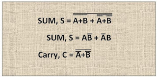
The NAND operation can be understood more clearly with the help
of equation given below. These equations are written in the form of operation
performed by NAND gates.

Half Adder using NOR Gates
The NOR gate is also a universal gate. Thus, it can also be used
for designing of any digital circuit. The Half adder can be designed using 5
NOR gates. This is the minimum number of NOR gates to design half adder.

Firstly, three NOR gates are used in the designing and the
output from two of these NOR gates is given to fourth NOR gate. The output from
second NOR gate is given to the gate connected at the end. This will generate
the sum bit of the addition of two 1-bit numbers.
The operation of the above circuit diagram can be understood
more clearly with the help of equation. The sum bit and carry bit can be
written in terms of NOR operations performed by the logic gates.


 NAND gates only. b) NOR gates only.)
0 Comments